


Overview:
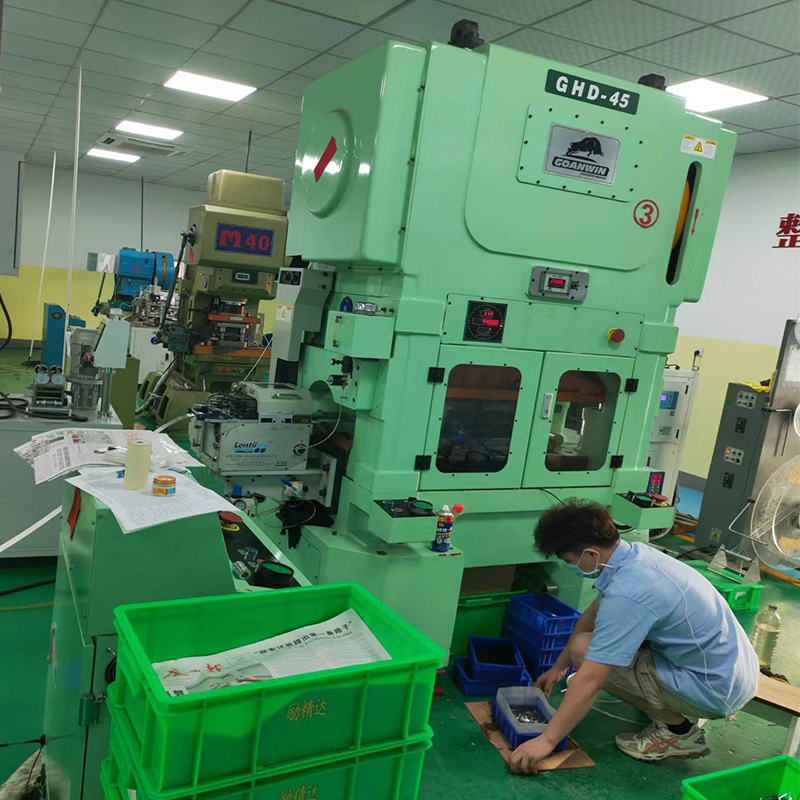
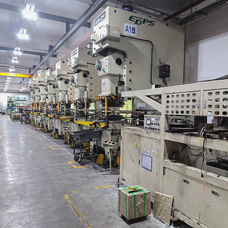
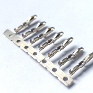
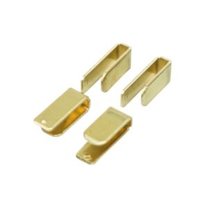
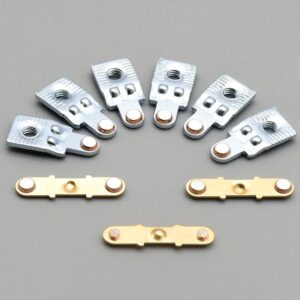
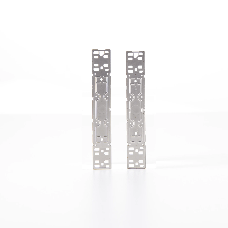
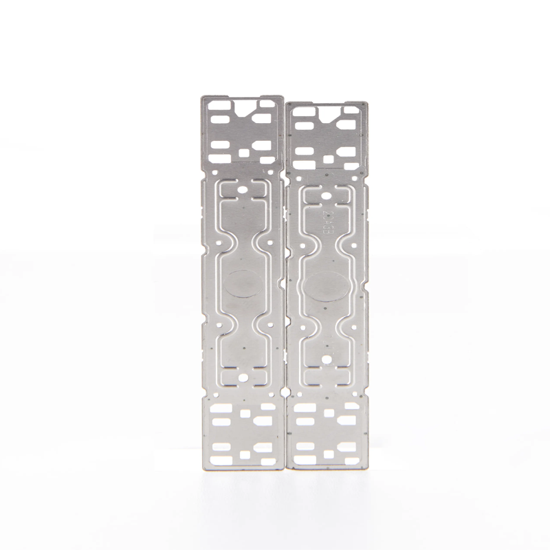
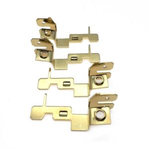
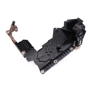
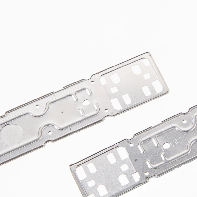
Semiconductor lead frames with metal etching are precision-engineered components used to support and connect semiconductor chips to external circuits. These frames are typically produced through advanced metal etching processes, which involve the selective removal of material to create highly detailed, intricate designs with tight tolerances. At our facility, we offer a one-stop service, from design and material selection to manufacturing and surface finishing. We maintain strict quality control throughout production to ensure optimal performance and reliability. Additionally, we provide sample production to meet your specific needs and guarantee satisfaction before mass production.
Features:
Processing Machinery: Suitable for Outdoor
Color: Silver / Custom
Material: Steel
Brand Name: OEM
Function: Notice
Design: Customized
Size: Custom Request
Sample Day: 5-7 Days
MOQ: 1000 PCS
Shape: Custom Shape
Styles: Decoration
Logo: Customized
Certification: ISO9001 / MSDS / CE
OEM: Yes
Thickness: Customized
Process: Etching, Silkscreen, Printing
Feature: Anti-UV, Waterproof
Export Market: Global
Transport Package: Standard Packaging
Specification: Customize
Origin: Xiamen, China
Production Capacity: 20,000 Pieces per Week
Advantages of Our Lead Frames:
– Design Flexibility:Our lead frames can be tailored to meet specific application requirements, allowing for versatile configurations.
– High Precision: Manufactured with advanced techniques, our lead frames ensure tight tolerances and accurate dimensions for optimal performance.
– Minimal Mold Costs: Our processes significantly reduce mold expenses, making production more cost-effective without compromising quality.
– Burr-Free Finish: Each lead frame undergoes rigorous quality control to ensure a smooth, burr-free surface, enhancing reliability.
– Short Lead Times: We prioritize efficiency, offering quick turnaround times to meet urgent production schedules and customer demands.
Etching Process
- Cleaning: The substrate is thoroughly cleaned to remove any contaminants and ensure optimal adhesion of the photoresist.
- Photoresist Coating: A uniform layer of photoresist material is applied to the cleaned substrate to create a sensitive surface for patterning.
- Exposure: The coated substrate is exposed to ultraviolet (UV) light through a mask, transferring the desired pattern onto the photoresist.
- Development: The exposed substrate undergoes a development process, where the photoresist is selectively removed, revealing the underlying material in the desired pattern.
- Etching: The exposed areas of the substrate are etched away using a chemical solution, creating the final design.
- Final Cleaning: A final cleaning step is performed to remove any remaining photoresist and etching residues, ensuring a pristine finish.
Our Advantages:
– Cost-Effective Tooling:We offer low tooling costs, eliminating the need for expensive dies or molds.
– Thin Metal Fabrication:Capable of processing a wide range of thin metals (thickness from 0.02 to 1.2 mm).
– No Additional Alteration Required: Our processes preserve the designer’s original specifications without the need for further modifications.
– Exceptional Accuracy:We ensure high precision in every component produced.
– Diverse Configurations: We can accommodate various apertures, shapes, and bar combinations tailored to your requirements.
– Burr and Stress-Free Manufacturing: Our methods minimize burrs and internal stresses, enhancing the quality of the final product.
– Rapid Prototyping: We provide quick turnaround times for prototypes to meet your specific needs.
– High Volume Production: Our capabilities support large-scale production while maintaining consistent quality.